Digital Imaging Camera/SDK
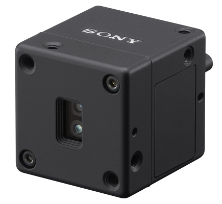
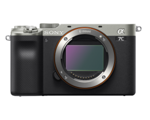
Sony Alpha camera supported by Sony SDK (Software Development Kit)
Sony Alpha camera supported by Sony SDK (Software Development Kit)
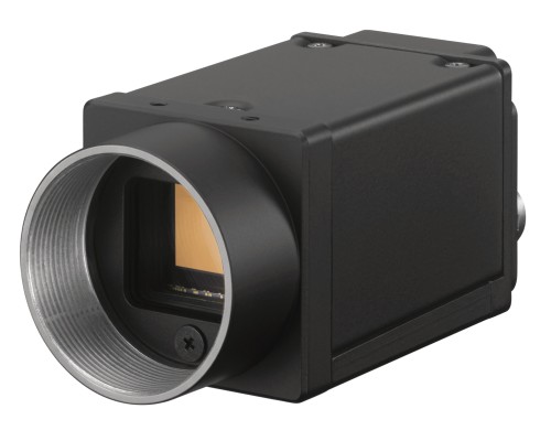
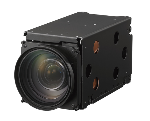
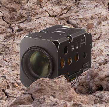
Digital Video Camera using various interfaces (USB, Gigabit Ethernet, Camera link)
Happy new year. Thank goodness 2020 is over and it’s a delight to be thinking to 2021, to a year where we can (post a widely rolled-out vaccine) meet up again.
And with this in mind what should the industry be most excited about over the coming 12 months? For me, there are three key themes, more advanced sensor technologies, a closer interaction between software and hardware, and a move towards larger sensors. My top 5 for 2021 are:
1. SWIR / hyperspectral imaging on CMOS
Industrial camera developers, such as Sony, need to do one thing - deliver images that can deliver as much information as possible. This has, for many years, focussed on the resolution - balancing pixel density and sensitivity. But, recent years have seen several big advances in sensor technology and that allows us to see so much more than just the visible spectrum.
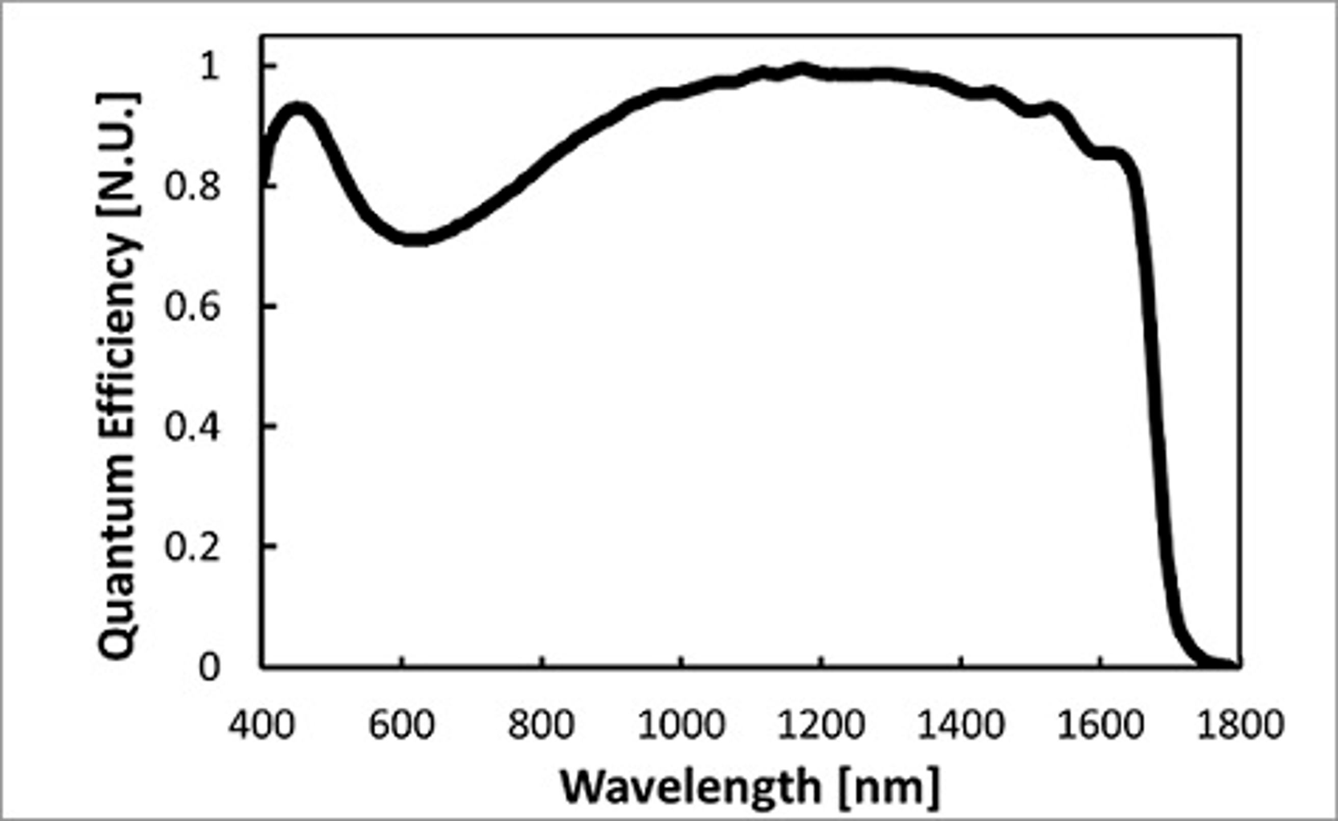
Last year Sony’s electronics division unveiled a big advance in hyperspectral sensors that enable both short wave infrared and visible light to be captured on a single sensor.
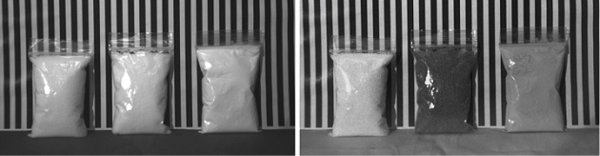
Description automatically generated
Additionally, it has done this on using CMOS, using a novel Cu-Cu bonding process, rather than the more costly InGaAs design, which allows a digital output on SWIR sensors for the first time.
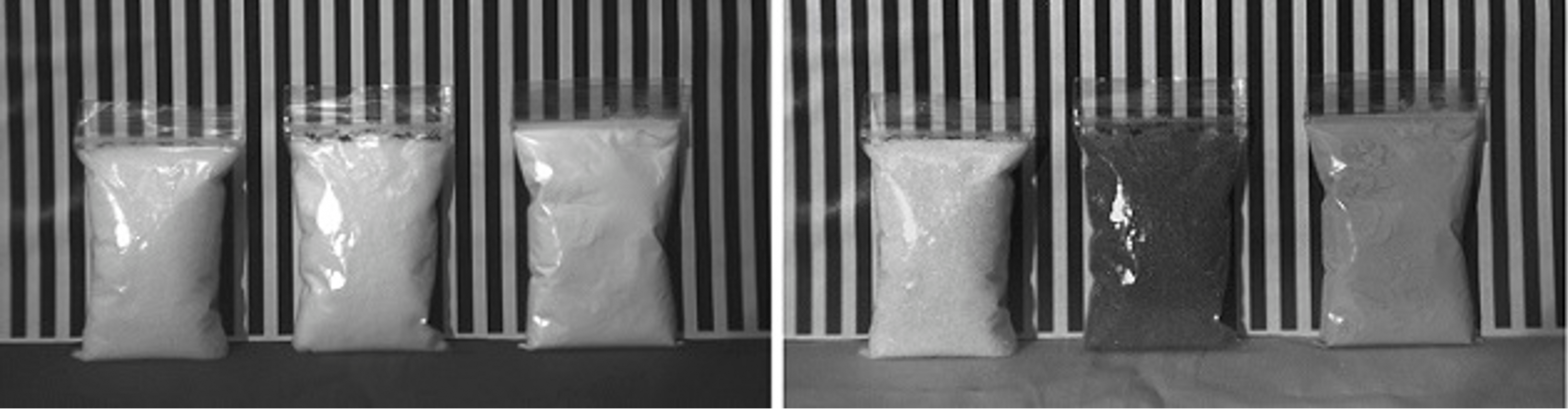
By using these it’s possible to sort materials more easily or spot contamination, I’ve used the salt vs sugar vs flour example in the image below, which all show up as white substances under visible light but reflect SWIR light very differently. It also allows other non-visible faults to be detected, including those below the skin… for example bruises in fruit and vegetables.
2. Depth information with advanced time of flight (ToF) sensors
Many industrial and B2B imaging applications demand depth information, be it an autonomous logistics robot, which needs it to travel safely through a warren-like warehouse; an augmented reality headset, which requires it to overlay information in the right place; a packing system, which uses this data to load containers more effectively or an building-site surveying system using it to detect environmental features or provide driver assistance when using diggers and other heavy machinery.
Recent advances in ToF sensors have allowed these to become far more accurate at both short and long range. And are able to give depth information at the pixel level.
This depth information (we feel) will prove vital for many customers in various applications.
3. Polarisation
Sony’s polarised sensors are already in production. In fact, on-chip polarisation (which incorporate polarisation at the pixel level) was the first to enter production, with the IMX250 launching in 2018 and with Sony ISS launching a camera and crucially an SDK for Windows providing pre-processing on polarised images in the same year.
Advances continue, and last year (2020) Sony added an SDK for the Nvidia Jetson, to enable applications that rely on AI capabilities, or those that need to use a compact computing platform.
Polarisation sensors provide unique capability to provide additional information on a scene, which the human eye cannot detect. It can help in difficult inspection tasks, where a subtle change, or the contamination of a material, needs to be detected; on the inspection of transparent objects; or to see through reflecting materials.

And resolutions are set to increase with Sony due to launch a 12 MP polarised sensor later this year.
4. Software and hardware will work more closely
In 2018 we developed our first imaging system SDK, which worked with our polarised camera - the XCG-CP510 to cut development time - a typical application might drop from 6 months to 6 weeks.
This was created in response to the unique skills needed for polarised cameras. But it showed us the need for such software that can be rolled out easily by system developers to get more from the camera.
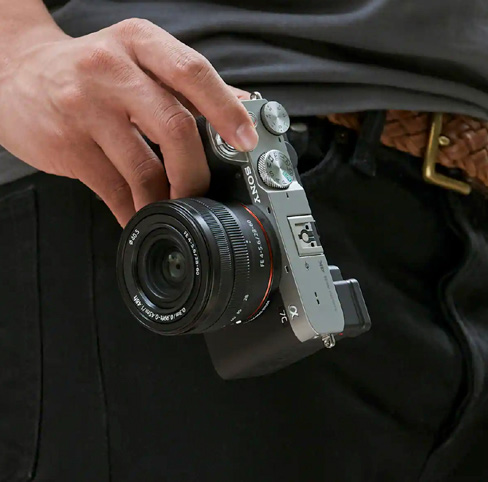
And we’re taking this further, with an SDK upgrade for Sony’s high-end digital still cameras (Alpha range) just launched - allowing these full-frame cameras to be automated to create multi camera systems, or have them used in ITS, security, drone and e-commerce systems. With this SDK, industrial customers can access the unique capabilities of these cameras, such as 61 Mp still image (even up to 240 megapixels combined image), or extreme sensitivity and dynamic range on 4K60 videos.
This concept will continue to evolve.
5. Improved resolutions without sacrificing sensitivity
Going full circle, we as an industry need to create cameras that give more information. And as well as the ability to see more than we can with the naked eye, the evolution of sensors for visible light is also continuing to enable improved resolutions…
There are two basic ways to improve resolutions - increase the size of the sensor, or increase pixel density.
On the first point, we’re going to be moving our cameras to use the larger 1/2” security sensors or even APS-C and full-frame sensor in the Sony Alpha camera range. This not only allows more pixels, but also larger pixels, which in turn allows more light to reach each pixel and extend dynamic range
On the second point, 2020 saw the development of fourth-generation global shutter CMOS sensors. Generations one to three have used the same sensor design and adjusted the pixel size to balance resolution and sensitivity - for example, third-generation GS CMOS sensors reduced the resolution vs the second generation. For the fourth generation a new topology was created, which flipped the sensor’s design to move the photosensitive layer above the copper wire layer.
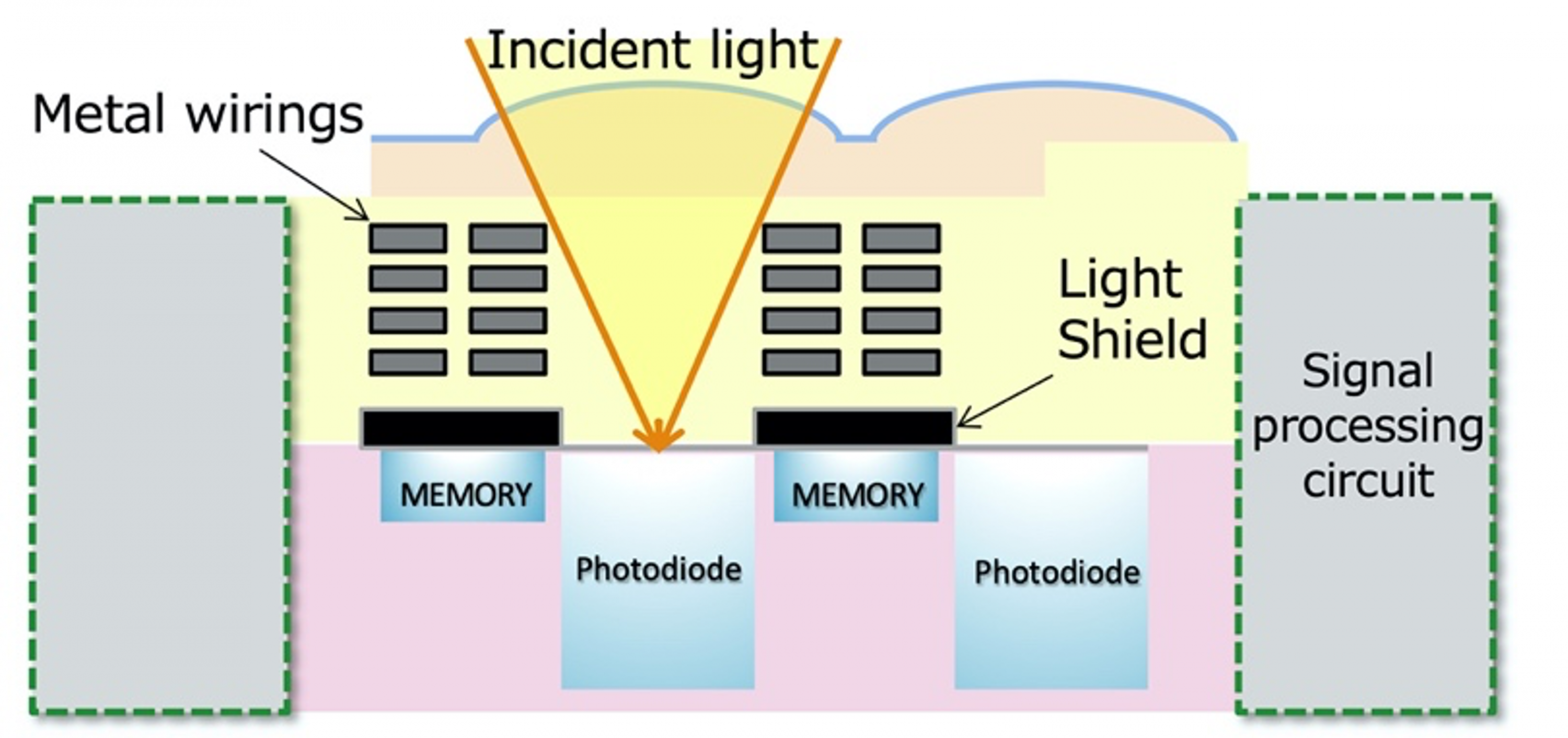
In doing this we increase the amount of light reaching the photosensitive layer (rather than being blocked by the copper wiring), the result is the ability to shrink the pixel without reducing the sensitivity vs third generation GS CMOS sensors.
Finally
Covid-19 - and the inability to take a demonstration to a customer - has forced us to undertake novel marketing approaches to demonstrate that our systems can do what we say they will. Over the coming months we will be rolling out videos that show the technology in action.
As I said at the beginning, we’re really looking forward to events like Vision where we can meet up with customers, but please do watch out for these videos. The first of which is below. We’d love your feedback.